Associate Professor
Jeehwan Kim
Interests
- 2D material-based layer transfer
- Neuromorphic Computing
- Nanoscale thin film flexible electronics/photonics
Professor Kim News + Media
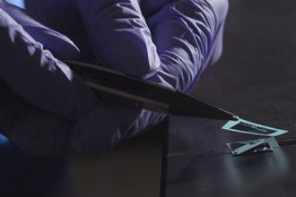
Next Generation Electronics
Jeehwan Kim, associate professor of mechanical engineering at MIT, is using his background in materials science to build a physical neural network and produce cheap semiconductor wafers – technologies that could help bring the artificial intelligence power of super computers to handheld devices.
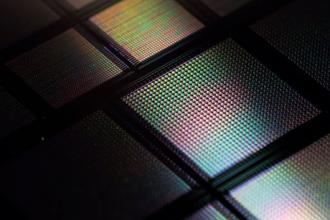
Engineers put tens of thousands of artificial brain synapses on a single chip
A team of researchers led by Associate Professor Jeehwan Kim have designed a “brain-on-a-chip” smaller than a piece of confetti that could advance the development of small portable AI devices.
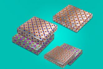
Engineers mix and match materials to make new stretchy electronics
Associate Professor Jeehwan Kim has developed a new process that may be the key to manufacturing flexible electronics with multiple functionalities in a cost-effective way.
Faculty Details
Education
-
MSE
UNIVERSITY OF CALIFORNIA-LOS ANGELES
Ph.D. -
MSE
SEOUL NATIONAL UNIVERSITY
M.S. -
MSE
Hongik University
B.S.
Research Interests
-
Neuromorphic computing
‐ 1R-based ANN arrays for online training/inference
- Artificial synapses based on single-crystalline ReRAM
-
Remote epitaxy, Graphene-based layer transfer
‐ III-V/III-N MicroLEDs
- Freestanding InGaAs-based IR Photodectors
- Freestanding Multifunctional complex oxides for magnetoelectric coupling
- SiC/IIII-N power electronics
-
Renewable energy, Energy storage
- Wafer recycling technique for GaAs solar cells based on remote epitaxy
- High efficiency III-V multi-junction solar cells based on remote epitaxy
- Single-crystalline all solid-state battery
-
Heterointegration, Flexible electronics
- Skin strain sensor arrays
- Flexible/transparent microLEDs
- Self-powered IoT system
-
Two-dimensional materials
- Monolayer-by-monolayer splitting of wafer‐scale 2D materials
- Wafer-scale single-crystalline 2D materials
- Wafer-scale 2D heterostructures
Online Data
- Selected News Coverages
- Nature News & Views: Materials Science: Crystals align through graphene
- MIT News: Not stuck on silicon
- EETimes: New Method Cuts Cost of GaAs Circuits
- IEEE Spectrum: Graphene Makes Infinite Copies of Compound Semiconductor Wafers
- MIT News: Researchers “iron out” graphene
- EETimes: IBM Conquers Wafer-Scale Graphene
- IBM Research News: First wafer-scale single-crystalline monolayer graphene
- IBM Research News: Growing single-crystalline materials on reusable graphene
- EETimes Europe: GaN for analog boosted by IBM tape lift-off
- Electronics Weekly: Will 2015 be the key year for graphene?
- Electronics Weekly: Graphene gets another real use – blue LED fabrication
- Semiconductor Today: Van der Waals epitaxy of GaN and blue LEDs
- Compound Semiconductor: Big Blue ambition
- Compound Semiconductor: US researchers use graphene to make flexible blue LEDs on plastic
Honors + Awards
- SENSE.nano Seed Grant, 2020
- DARPA Young Faculty Award, 2019
- U.S. Department of Energy Solar Energy Technologies Office Fiscal Year 2018 Funding Program, 2018
- IBM Faculty Award, 2016
- Lam Research Foundation Award, 2015, 2016
- Master Inventor of IBM Corporation, 2012
- 25 Invention Achievement Awards, IBM 2008-2015
- 15 High Value Patent Awards, IBM 2008-2015
Teaching
2.001 Mechanics and Materials
2.674 Micro/Nano Engineering Laboratory
2.671 Instrument and Measurement
Publications
- Selected Publications
-
1. Jaewoo Shim†, Sang-Hoon Bae†, Wei Kong†, Doyoon Lee†, Kuan Qiao et al., and Jeehwan Kim*, “Controlled crack propagation for atomic precision handling of wafer-scale two-dimensional materials” Science (2018)
- 2. Wei Kong†, Huashan Li†, Kuan Qiao†, Yunjo Kim, Kyusang Lee, Yifan Nie, Doyoon Lee, et al., Jeffrey C. Grossman*, and Jeehwan Kim*, "Polarity governs atomic interaction through two-dimensional materials", Nature Materials (2018)
-
3. S. Choi, S. Tan, Z. Li, Y. Kim, C. Choi, P.-Y Chen, S. Yu, and Jeehwan Kim*, “SiGe epitaxial memory for neuromorphic computing with reproducible high performance based on engineered dislocations,” Nature Materials (2018)
-
4. Y. Kim, S. S. Cruz, K. Lee, B. O. Alawode, C. Choi, Y. Song, J. M. Johnson, C. Heidelberger, W. Kong, S. Choi, K. Qiao, E. A. Fitzgerald, J. Kong, A. M. Kolpak, J. Hwang, and Jeehwan Kim*, “Remote epitaxy through graphene: Role of underlying substrates on van der Waals epitaxy” Nature, Vol. 544, 340–343 (2017) featured as a cover
-
5. S.‐H. Bae, X. Zhou, S. Kim, Y. S. Lee, S. Cruz, Y. Kim, J. B. Hannon, Y. Yang, D. K. Sadana, F.s M. Ross, H. Park, and Jeehwan Kim*, “Unveiling the carrier transport mechanism in epitaxial graphene for forming wafer‐scale, single‐domain graphene,” Proceedings of the National Academy of Science, Vol. 114, 4082-4086 (2017)
- 6. Jeehwan Kim*, Can Bayram*, Hongsik Park, Cheng-Wei Cheng, Christos Dimitrakopoulos, John Ott, Kathleen Reuter, Stephen Bedell, and Devendra Sadana,“Principle of direct van der Waals epitaxy of single-crystalline films on epitaxial graphene”, Nature Communications, Vol. 5, 4836 (2014)
- 7. Jeehwan Kim*, Hongsik Park*, James B. Hannon, Stephen W. Bedell, Keith Fogel, Devendra K. Sadana, Christos Dimitrakopoulos*,“Layer-resolved graphene transfer via engineered strain layers”, Science, Vol. 342, 833 (2013)
Patents
- Selected US Patents
- 1. Grant # US 9,153,729 Atomic layer deposition for photovoltaic devices
- 2. Grant # US 9,123,842 Photoreceptor with improved blocking layer
- 3. Grant # US 9,123,838 Transparent conductive electrode for three dimensional photovoltaic device
- 4. Grant # US 9,105,854 Transferable transparent conductive oxide
- 5. Grant # US 9,105,805 Enhancing efficiency in solar cells by adjusting deposition power
- 6. Grant # US 9,099,664 Transferable transparent conductive oxide
- 7. Grant # US 9,096,050 Wafer scale epitaxial graphene transfer
- 8. Grant # US 9,093,290 Self-formation of high-density arrays of nanostructures
- 9. Grant # US 9,070,617 Reduced S/D contact resistance of III-V mosfet using low temperature metal-induced crystallization of n+ Ge
- 10. Grant # US 9,059,272 Self-aligned III-V MOSFET fabrication with in-situ III-V epitaxy and in-situ metal epitaxy and contact formation
- 11. Grant # US 9,059,271 Self-aligned III-V MOSFET fabrication with in-situ III-V epitaxy and in-situ metal epitaxy and contact formation
- 12. Grant # US 9,059,013 Self-formation of high-density arrays of nanostructures
- 13. Grant # US 9,040,428 Formation of metal nanospheres and microspheres
- 14. Grant # US 9,040,340 Temperature grading for band gap engineering of photovoltaic devices
- 15. Grant # US 9,035,282 Formation of large scale single crystalline graphene
- 16. Grant # US 8,933,456 Germanium-containing release layer for transfer of a silicon layer to a substrate
- 17. Grant # US 8,927,857 Silicon: hydrogen photovoltaic devices, such as solar cells, having reduced light induced degradation and method of making such devices
- 18. Grant # US 8,916,451 Thin film wafer transfer and structure for electronic devices
- 19. Grant # US 8,916,409 Photovoltaic device using nano-spheres for textured electrodes
- 20. Grant # US 8,901,695 High efficiency solar cells fabricated by inexpensive pecvd
- 21. Grant # US 8,889,466 Protective insulating layer, chemical mechanical polishing for polycrystalline thin film solar cells
- 22. Grant # US 8,889,456 Method of fabricating uniformly distributed self-assembled solder dot formation for high efficiency solar cells
- 23. Grant # US 8,878,055 Efficient nanoscale solar cell and fabrication method
- 24. Grant # US 8,866,003 Solar cell employing an enhanced free hole density p-doped material and methods for forming the same
- 25. Grant # US 8,859,321 Mixed temperature deposition of thin film silicon tandem cells
- 26. Grant # US 8,846,440 Germanium photodetector
- 27. Grant # US 8,841,544 Uniformly distributed self-assembled solder dot formation for high efficiency solar cells
- 28. Grant # US 8,841,162 Germanium photodetector
- 29. Grant # US 8,828,504 Deposition of hydrogenated thin film
- 30. Grant # US 8,822,317 Self-aligned III-V MOSFET diffusion regions and silicide-like alloy contact
- 31. Grant # US 8,735,210 High efficiency solar cells fabricated by inexpensive PECVD
- 32. Grant # US 8,685,858 Formation of metal nanospheres and microspheres
- 33. Grant # US 8,679,947 Self-formation of high-density defect-free and aligned nanostructures
- 34. Grant # US 8,653,360 Compositionally-graded band gap heterojunction solar cell
- 35. Grant # US 8,642,431 N-type carrier enhancement in semiconductors
- 36. Grant # US 8,628,999 Solar cell made in a single processing chamber
- 37. Grant # US 8,628,996 Uniformly distributed self-assembled cone-shaped pillars for high efficiency solar cells
- 38. Grant # US 8,624,361 Self-formation of high-density defect-free and aligned nanostructures
- 39. Grant # US 8,617,938 Device and method for boron diffusion in semiconductors
- 40. Grant # US 8,614,116 Germanium photodetector
- 41. Grant # US 8,536,043 Reduced S/D contact resistance of III-V MOSFET using low temperature metal-induced crystallization of n+ Ge
- 42. Grant # US 8,476,152 N-type carrier enhancement in semiconductors
- 43. Grant # US 8,354,694 CMOS transistors with stressed high mobility channels
- 44. Grant # US 8,343,863 N-type carrier enhancement in semiconductors
- 45. Grant # US 8,304,272 Germanium photodetector
- 46. Grant # US 8,298,923 Germanium-containing release layer for transfer of a silicon layer to a substrate
- 47. Grant # US 8,178,430 N-type carrier enhancement in semiconductors
- 48. Grant # US 8,039,371 Reduced defect semiconductor-on-insulator hetero-structures
- 49. Grant # US 7,935,612 Layer transfer using boron-doped SiGe layer
- 50. Grant # US 7,754,008 Method of forming dislocation-free strained thin films