Closing the design-to-manufacturing gap for optical devices
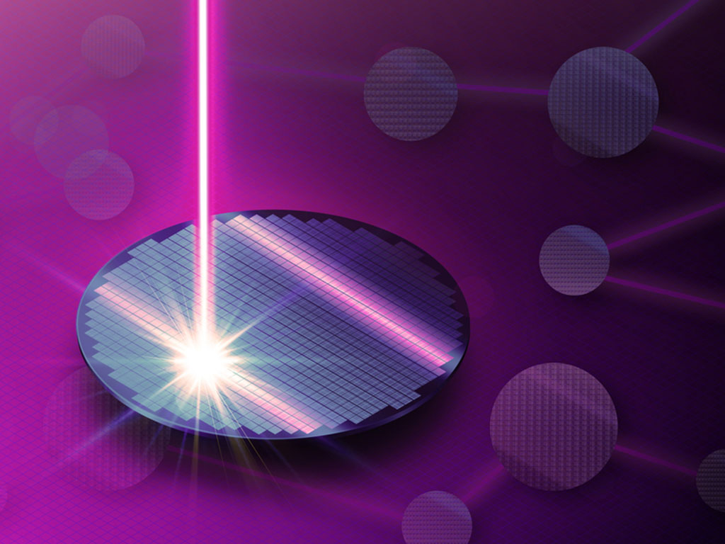
Photolithography involves manipulating light to precisely etch features onto a surface, and is commonly used to fabricate computer chips and optical devices like lenses. But tiny deviations during the manufacturing process often cause these devices to fall short of their designers’ intentions.
To help close this design-to-manufacturing gap, researchers from MIT and the Chinese University of Hong Kong used machine learning to build a digital simulator that mimics a specific photolithography manufacturing process. Their technique utilizes real data gathered from the photolithography system, so it can more accurately model how the system would fabricate a design.
The researchers integrate this simulator into a design framework, along with another digital simulator that emulates the performance of the fabricated device in downstream tasks, such as producing images with computational cameras. These connected simulators enable a user to produce an optical device that better matches its design and reaches the best task performance.
This technique could help scientists and engineers create more accurate and efficient optical devices for applications like mobile cameras, augmented reality, medical imaging, entertainment, and telecommunications. And because the pipeline of learning the digital simulator utilizes real-world data, it can be applied to a wide range of photolithography systems.
“This idea sounds simple, but the reasons people haven’t tried this before are that real data can be expensive and there are no precedents for how to effectively coordinate the software and hardware to build a high-fidelity dataset,” says Cheng Zheng, a mechanical engineering graduate student who is co-lead author of an open-access paper describing the work. “We have taken risks and done extensive exploration, for example, developing and trying characterization tools and data-exploration strategies, to determine a working scheme. The result is surprisingly good, showing that real data work much more efficiently and precisely than data generated by simulators composed of analytical equations. Even though it can be expensive and one can feel clueless at the beginning, it is worth doing.”
Zheng wrote the paper with co-lead author Guangyuan Zhao, a graduate student at the Chinese University of Hong Kong; and her advisor, Peter T. So, a professor of mechanical engineering and biological engineering at MIT. The research will be presented at the SIGGRAPH Asia Conference.
Printing with light
Photolithography involves projecting a pattern of light onto a surface, which causes a chemical reaction that etches features into the substrate. However, the fabricated device ends up with a slightly different pattern because of miniscule deviations in the light’s diffraction and tiny variations in the chemical reaction.
Because photolithography is complex and hard to model, many existing design approaches rely on equations derived from physics. These general equations give some sense of the fabrication process but can’t capture all deviations specific to a photolithography system. This can cause devices to underperform in the real world.
For their technique, which they call neural lithography, the MIT researchers build their photolithography simulator using physics-based equations as a base, and then incorporate a neural network trained on real, experimental data from a user’s photolithography system. This neural network, a type of machine-learning model loosely based on the human brain, learns to compensate for many of the system’s specific deviations.
The researchers gather data for their method by generating many designs that cover a wide range of feature sizes and shapes, which they fabricate using the photolithography system. They measure the final structures and compare them with design specifications, pairing those data and using them to train a neural network for their digital simulator.
“The performance of learned simulators depends on the data fed in, and data artificially generated from equations can’t cover real-world deviations, which is why it is important to have real-world data,” Zheng says.
Dual simulators
The digital lithography simulator consists of two separate components: an optics model that captures how light is projected on the surface of the device, and a resist model that shows how the photochemical reaction occurs to produce features on the surface.
In a downstream task, they connect this learned photolithography simulator to a physics-based simulator that predicts how the fabricated device will perform on this task, such as how a diffractive lens will diffract the light that strikes it.
The user specifies the outcomes they want a device to achieve. Then these two simulators work together within a larger framework that shows the user how to make a design that will reach those performance goals.
“With our simulator, the fabricated object can get the best possible performance on a downstream task, like the computational cameras, a promising technology to make future cameras miniaturized and more powerful. We show that, even if you use post-calibration to try and get a better result, it will still not be as good as having our photolithography model in the loop,” Zhao adds.
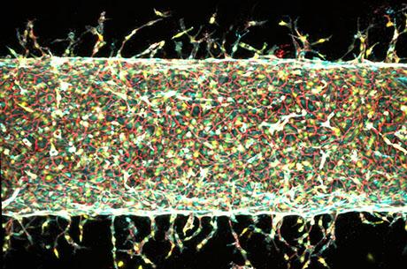
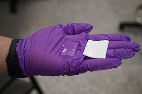
They tested this technique by fabricating a holographic element that generates a butterfly image when light shines on it. When compared to devices designed using other techniques, their holographic element produced a near-perfect butterfly that more closely matched the design. They also produced a multilevel diffraction lens, which had better image quality than other devices.
In the future, the researchers want to enhance their algorithms to model more complicated devices, and also test the system using consumer cameras. In addition, they want to expand their approach so it can be used with different types of photolithography systems, such as systems that use deep or extreme ultraviolet light.
This research is supported, in part, by the U.S. National Institutes of Health, Fujikura Limited, and the Hong Kong Innovation and Technology Fund.